Internals of Apple Watch’s S1 Chip Reveal Unexpected Suppliers
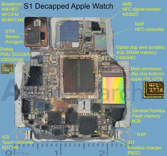
While Chipworks has previously offered an early look at the chip’s internals using x-ray imaging, the folks over at ABI Research have now taken the Apple Watch’s S1 chip completely apart, revealing a number of components that have previously not been identified (via MacRumors). The following photo of the chip’s internals reveals the main processor at the centre carrying part number APL 0778, with 4 Gb (512 MB) of Elpida SRAM on top, among other components.

The S1 also packs an 8 GB flash storage chip, a Broadcom Wi-Fi chip, an accelerometer / gyroscope from STMicroelectronics instead of the previously predicted InvenSense, touch controllers from ADI which were also unexpected, and a wireless charging chip from IDT that facilitates the Apple Watch’s inductive charging.
“The design is an obvious variation from Apple’s smartphones, with many high-end functions / chips included that normally would not be found in a simple watch,” comments Jim Mielke, VP Engineering at ABI Research and head of the TeardownIQ group. “Judging by the complexity of the printed circuit board (PCB), and the number of parts on the PCB, one might think the Apple watch is a full-fledged cellular connected watch but in fact connectivity is limited to Wi-Fi, Bluetooth, and NFC.”
Any yet, the S1 chip takes only a small percentage of space inside the Apple Watch chassis, while majority of space is taken up by the battery and Taptic Engine / speaker assembly.

