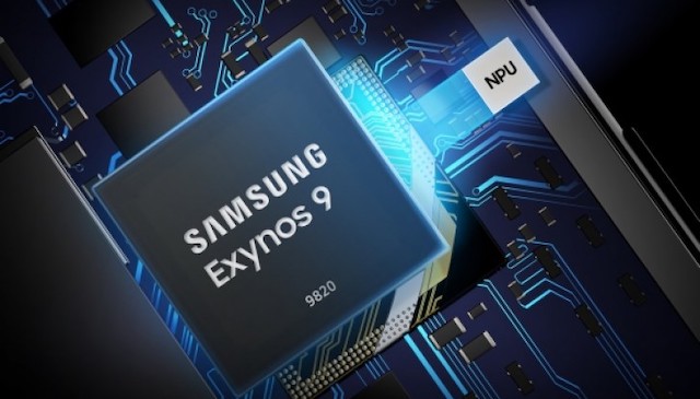
Samsung’s $116 Billion Investment Aimed at Global Chip Supremacy
Earlier this year, Samsung announced a 10-year, $116 billion plan to take over the lead as the world’s foremost processor maker by 2030 and today, Bloomberg has revealed how the South Korean company is investing heavily in extreme ultraviolet lithography (EUV), the next step in miniaturizing semiconductors.

“The complexity of the lines drawn by the EUV equipment is similar to building a spaceship,” said Samsung’s foundry business president ES Jung. A single EUV machine costs $172 million and Samsung is setting up dozens of them in Hwaseong in an effort to be first with the technology.
The publication notes that Samsung executives are touring major cities from San Jose to Munich to Shanghai to win over clients, hosting foundry forums and negotiating deals:
“A new market is opening up,” Yoon Jong Shik, executive vice president of Samsung’s foundry business, said at a forum recently held in Seoul. “Companies like Amazon, Google, and Alibaba, which lack experience in silicon design, are seeking to make chips with their own concept ideas in order to boost their services. I think this would bring a significant breakthrough for our non-memory chip business.”
Samsung has already agreed to sell 5G Exynos chips to Vivo and also to manufacture Qualcomm’s 5G mobile chipset using the same EUV process.

