A6 Teardown Reveals Dual ARM Cores, Three Graphics Cores [PICS]
We have previously seen diffusion images of Apple’s new dual core A6 processor, but now iFixit and Chipworks have teamed up to perform a much more thorough tear down of the new Apple-designed chip using an ion blaster, a process comparable to “sandblasting a chip to remove specific layers. Instead of sand, though, Ibe uses the atoms in an ion beam to do its dirty work.”
AnandTech previously noted the A6 chip was custom-designed by Apple and the teardown reveals this, along with confirmation the new processor utilizes Samsung’s 32 nm CMOS process, which we have seen in newer iPad 2 units and the 3rd generation Apple TV (which leads to better battery life):
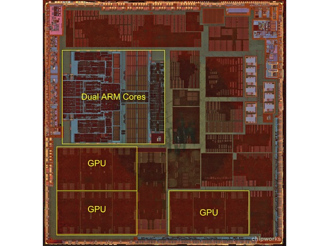
Samsung isn’t completely absent in the A6, though. The Apple A6—labeled APL0598 on the package marks and APL0589B01 on the inside—is fabricated by Samsung on their 32 nm CMOS process and measures 9.70 mm x 9.97 mm.
Check out the image of the A6 below, detailing the Apple-customized layout of dual cores and three GPUs:
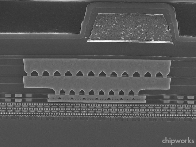
Here’s a cross cut image of the A6:
The raised mesa-looking shapes in the magnified cross-section view (second image) are the transistors’ structures, and the little pegs running between them are the actually the contacts between layers.
Early benchmarks of the iPhone 5 have shown it performs better than all competitors, taking the current title as the ‘fastest smartphone ever’. How are you enjoying the performance of your iPhone 5?


