The iPhone 6’s A8 CPU Gets Teardown Treatment to Transistor Level [PICS]
While IHS’ teardown gave us an estimate of the raw bill of materials Apple needs to pay for each iPhone it manufactures, the guys from Chipworks continued their own dive into the latest iPhones, revealing other tidbits, such as a dive-level shot of the A8 chip, and confirming further rumours about Sony and others.
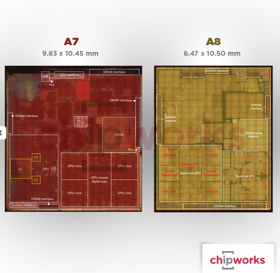
The A8 chip has a die size of 89.25 sq. mm (8.5 mm x 10.5 mm), and every sign points to TSMC (but according to IHS, Samsung has about 40% of the orders). The CPU is still dual-core, but it has an area of 12.2 sq. mm, versus the 17.2 sq. mm in the A7.
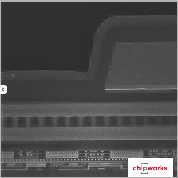
There has been much comment that the die is notably smaller than the A7, at 89 mm2 vs. 104 mm2, or 85% of the A7 area, yet with two billion transistors vs “over a billion”. If we take the 28 ->20-nm node size reduction, then with the same functionality the shrink of the die area should be to ~51% of the A7 size, or ~53 mm2. Clearly at 89 mm2, there is quite a bit of extra power added into the die.
If we look at the CPU, it is still a dual-core, but now has an area of 12.2 mm2 vs. 17.1 in the A7, or 71%; so again, more functionality added. Ryan speculates that it is a tweaked version of the A7’s Cyclone CPU. Looking at the two core layouts, it may be that each core has its own L2 cache, as opposed to the shared cache of the A7, and it is also possible that both the L1 and L2 caches are larger, up from 256 KB and 1 MB respectively.
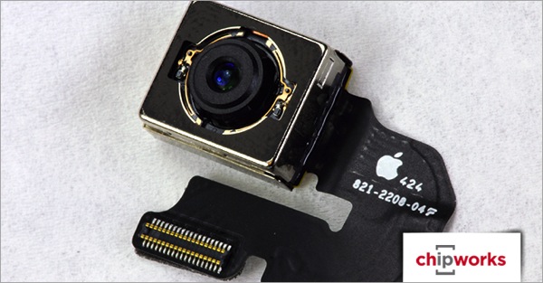
As for the iSight camera, Apple has decided to challenge camcorders this time (after successfully challenging point-and-shoot cameras in the past). The iPhone 6’s iSight camera chip is a stacked Exmor RS, back-illuminated CMOS image sensor featuring 1.5 µm generation pixels with a die size of 4.8 mm x 6.1 mm (29.3 sq. mm).
Also: Remember those rumours of Sony winning the contract for the FaceTime camera sensors? As it turns out, they were true — Chipworks can confirm it.
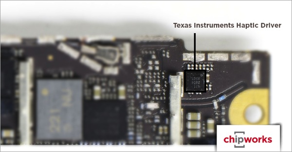
The teardown also revealed the Texas Instruments DRV2604 haptic driver on the main board, used to drive the vibrator on both iPhones.
This is only the preliminary report of the iPhone 6 and iPhone 6 Plus teardown. Stay tuned, and we’ll keep you posted.
